New Japanese Material Promises AI Chips 1000x Faster
As tech giants like Nvidia, OpenAI, and Microsoft engage in an infrastructure arms race, battling the massive energy consumption and heat of modern data centers, the real solution to the AI bottleneck might just have emerged from a Japanese lab.
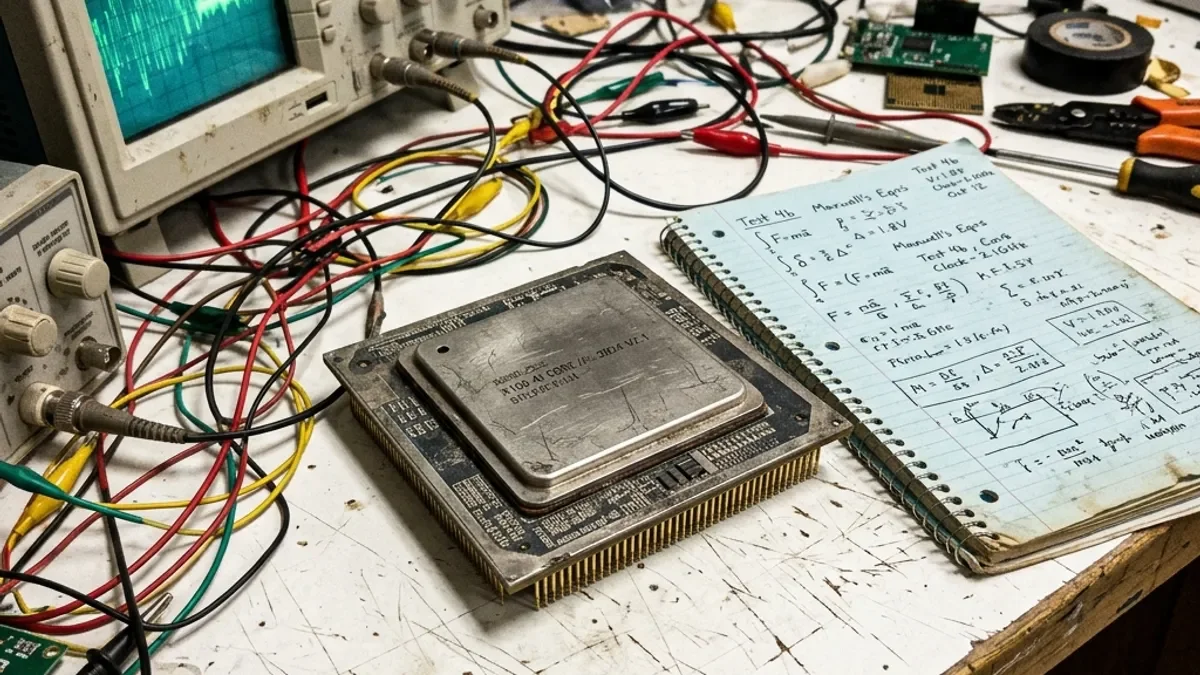
A study published in the prestigious journal Science on May 14, 2026 (UTC), led by researchers from the University of Tokyo, unveiled a memory and processing device based on a topological antiferromagnetic material (manganese-tin, or Mn₃Sn) that operates about 1,000 times faster than current CPU and GPU technologies.
The "Holy Grail" of AI Computing
The major challenge in AI today isn't just software, but thermodynamics. Modern chips operate on the nanosecond scale using traditional electrical currents, generating enormous heat that demands industrial-scale cooling systems (often compared to nuclear power plant consumption).
The Japanese device, developed by a team including researchers Hanshen Tsai, Takuya Matsuda, and Professor Satoru Nakatsuji, uses spintronics (specifically, spin-orbit torque). Instead of moving electrons to represent bits (0 and 1), it utilizes the "spin" property of electrons. The result? The magnetic state can be rewritten in 40 picoseconds with electrical pulses and an impressive 60 picoseconds via photocurrent (using optical signals), with energy consumption several orders of magnitude lower and almost no heat generation.
From Hours to Seconds
The direct implication for Artificial Intelligence is monumental. The device is non-volatile, meaning it retains information without needing constant power. For data centers training LLMs (Large Language Models), this means massive matrix computations could be performed without the thermal "meltdown" of conventional GPUs.
According to the study's projections, complex computational processes that currently take 1 hour to complete could theoretically be executed in about 1 second on architectures based on this material. The team also demonstrated photoelectric conversion — transforming an optical signal (laser) directly into an electric one to write to memory — a giant leap for integrating optoelectronics and spintronics on the same chip.
The Path to Data Centers
While the discovery marks a historic advancement for material physics and topological computing, Mn₃Sn-based chips are still in the lab phase. The University of Tokyo, in partnership with institutions like the RIKEN institute, aims to scale the technology to practical industrial prototypes by around 2030.
Until then, the discovery published in Science (DOI: 10.1126/science.adt3136) serves as proof of concept that the solution to AI's energy hunger won't just be building more nuclear plants, but fundamentally rethinking hardware physics.
This content was created and reviewed by our team (iatoskill.com), if you find any issues, please reach out to us